

 - EN
 - EN
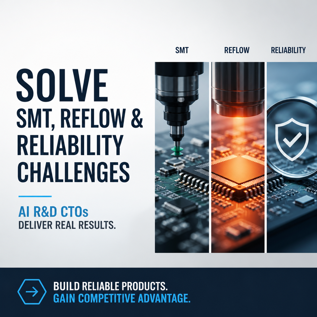
The barrier isn’t “assembly”—it’s repeatability:
SMT teams rarely struggle with placing components. They struggle with repeatable outcomes when real-world variation hits: paste volume drift, warped PCBs, mixed-mass heating, marginal component terminations, and firmware/hardware interactions that only appear after thermal cycling. These issues show up as bridging, voiding, head-in-pillow, tombstoning, intermittent opens, and field returns that are hard to reproduce.
An AI R&D CTO helps a local engineering team step outside the day-to-day bubble. The goal is not generic “AI advice,” but world-class technical intelligence: proven design patterns, process variables worth testing, known failure modes, and experiment designs that turn reliability chaos into an engineering decision.
When your technical objective is stable solder joints and robust manufacturability, you typically hit an unexpected barrier—like thermal gradients causing brittle intermetallic formation or EMI-driven resets that appear only after reflow-induced microcracks. When the current approach fails, the team needs alternatives, structured experiments, and a disciplined record of what changed and why.
SMT defects as engineering hypotheses: bridging, voiding, warpage, and solder-joint quality:
A practical way to SOLVE SMT defects is to treat every defect mode as a hypothesis about physics, materials, and process interactions.
For bridging and solder balling, the AI R&D CTO can guide the team to investigate variables that often dominate outcomes: stencil thickness and aperture reductions, paste type selection (metal load, flux chemistry), squeegee pressure/speed, under-stencil cleaning frequency, and component pitch-to-aperture geometry.
For voiding, the intelligence layer can surface proven levers: soak time changes, peak temperature optimization, vacuum reflow feasibility, paste formulation tradeoffs, and pad design modifications that influence outgassing pathways. For warpage and head-in-pillow, the focus shifts to package/PCB CTE mismatch, board support tooling, reflow profile slope control, and paste deposition consistency.
Instead of guessing, the AI Technical Advisor role helps the team outline an experimental plan: define defect metric (x-ray void %, AOI bridge rate), isolate controllable variables, run controlled trials, and compare results against acceptance thresholds. This is also where manufacturability improves—because the team isn’t just fixing one build; it’s building process capability.
Reflow profiling as a controlled experiment: thermal behavior, mixed-mass boards, and component reliability:
Reflow is frequently where “it should work” turns into “it fails intermittently.” Mixed-mass assemblies create thermal lag: large BGAs and connectors heat slowly while small passives race to liquidus. Overcorrecting can damage components or degrade solder alloy behavior.
An AI R&D CTO can pull in cross-industry tactics and academic research signals to propose actionable experiments:
– Profile segmentation: tuning preheat ramp to reduce solder spatter and tombstoning, then refining soak to equilibrate mixed-mass temperatures.
– Time above liquidus (TAL): experimenting with TAL windows to reduce voiding while avoiding excessive intermetallic growth that can embrittle joints.
– Peak temperature spread: minimizing delta-T across the PCB using fixture/support adjustments and oven zone balancing.
– Atmosphere considerations: nitrogen vs. air tradeoffs when dealing with oxidation-sensitive terminations.
The core pattern is consistent: technical objective → unexpected thermal barrier → current profile fails → alternatives must be identified → experiments are designed → results compared → next technical decision is made. This is also prime territory for documenting Qualified Research Activities (QRAs) because the work is resolving technical uncertainty through a process of experimentation.

“AI unlocks the value in your data.”
– Arvind Krishna, Chairman and CEO of IBM
Signal integrity, EMI, and “works-on-the-bench” failures: PCB redesign + firmware changes:
Reliability issues aren’t always solder defects. Many electronics failures trace back to signal integrity and EMI interactions that are amplified by assembly realities.
Examples your team may recognize:
– A board passes functional test, but fails in the field after thermal cycling—microcracks change impedance or create intermittent ground bounce.
– High-speed interfaces degrade after a layout revision—via stubs, return path discontinuities, or poor reference plane integrity cause eye closure.
– A device resets only during certain load transients—EMI couples into reset lines or power integrity dips below brownout thresholds.
Here, the AI Product Intelligence and AI Innovation Platform concept is applied to R&D decision-making (not to your product). The AI R&D CTO can scan for relevant design patterns: stackup choices for controlled impedance, decoupling network strategies, spread-spectrum clocking tradeoffs, shielding/grounding approaches, and known failure modes for specific component families.
Just as important, the AI Product Strategy layer helps coordinate the “hardware + embedded firmware” response: filtering and debounce strategies, watchdog tuning, power sequencing changes, and diagnostic telemetry to reproduce edge cases. That combination—PCB redesign plus embedded firmware changes to resolve hardware interaction problems—often creates the fastest path from mystery to measurable improvement.
From rework to reliability: proving manufacturability with accelerated stress and root-cause workflows:
Electronics reliability becomes real when the team can predict performance under stress: thermal cycling, vibration, humidity, and power cycling. The barrier is often component reliability and solder-joint fatigue that only appears after repeated expansion/contraction.
An AI R&D CTO can help the team create a root-cause workflow that ties defects to mechanisms:
– Failure analysis planning (cross-section, x-ray, dye-and-pry, microsectioning criteria)
– Hypothesis mapping (e.g., voiding → localized hot spots → early fatigue)
– Test design (accelerated thermal cycling profiles that reflect field conditions)
– Comparison logic (baseline vs. modified stencil/paste/profile/layout)
This “prove it” approach is what transforms firefighting into Innovation Management. It also produces the kind of contemporaneous technical documentation the IRS or CRA expects when evaluating whether work meets the four-part test or eligibility for Research and Development Tax Credits.
How an AI R&D CTO streamlines R&D Tax Credit claims for electronics experimentation:
When teams are genuinely experimenting to resolve technical uncertainty—bridging, voiding, warpage, thermal behavior, EMI, signal integrity, component reliability, solder-joint quality, and manufacturability—those efforts may qualify for R&D Tax Credits.
Traditional R&D Tax Credit Services often rely on manual interviews, after-the-fact narratives, and spreadsheets. An AI R&D CTO replaces much of that manual lift by guiding documentation in parallel with engineering work—improving precision and reducing disruption.
Using sector-specific trained LLMs for electronics and PCB contexts, the AI R&D CTO can help:
– Identify Qualified Research Activities aligned to reflow profiling trials, stencil experiments, PCB redesign iterations, and firmware mitigation testing.
– Clarify technical uncertainties: why the outcome couldn’t be known at the outset (e.g., voiding sensitivity to TAL vs. paste chemistry).
– Capture experimentation: variables tested, test methods, data comparisons, and conclusions.
– Support Qualified Research Expenses (QREs) estimates by mapping time and resources to the experimental work.
– Produce an R&D Study package that supports IRS compliance, including contemporaneous notes, technical summaries, and project narratives.
The output supports Form 6765 preparation and can improve Business Cash Flow through an R&D Tax Credit Refund or reduced tax liability—turning documented experimentation into Tax Savings. In short: SOLVE the reliability problem while FUNDING the next iteration.
R&D Tax Credit readiness for SMT and reliability work: what to capture while you build:
Electronics teams move fast; documentation lags. A lightweight capture discipline makes Research and Development Tax Credits far easier later.
A practical framework the AI Technology Advisor can enforce during active builds includes:
– Objective: the measurable goal (e.g., reduce BGA voiding below X%, eliminate intermittent resets)
– Uncertainty: what was unknown (process window, design margin, material interaction)
– Alternatives: what approaches were considered (profile changes, stencil redesign, layout changes)
– Experiments: runs, variables, and methods (AOI/X-ray criteria, thermal profiles, stress tests)
– Results: comparisons and what changed next
This becomes the backbone of a defensible R&D Study while simultaneously improving engineering decision velocity. For many startups, software companies building embedded systems, manufacturers, and engineering firms, these records unlock overlooked R&D Tax Credit eligibility.
Next: make your tax credit a self-funding innovation engine:
SHAIN’s AI R&D CTO positioning is simple: democratize innovation by combining R&D Tax Credit intelligence with world-class technical guidance. You get Virtual CTO-level support (AI Chief Technology Officer capability) focused on solving SMT, reflow, and electronics reliability barriers—while also strengthening your Research and Development Tax Credits position through better evidence, cleaner narratives, and clearer QRE mapping.
To learn more about how an AI R&D CTO can enhance knowledge to world-class standards while seamlessly gaining R&D Tax Credits—and to get an estimate of how much your R&D Tax Credit could be—select the button below.