

 - EN
 - EN
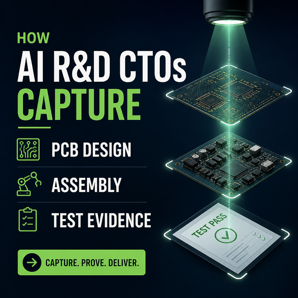
Automate Preparation, Support and Compliance of R&D Tax Credits:
Electronics teams already generate a mountain of engineering artifacts—schematics, Gerbers, BOMs, reflow profiles, bench logs, firmware commits, and failure reports. The problem is not simply “having documents.” The real problem is proving what happened, why it was technically uncertain, what was tested, who participated, and how the supporting records connect to an R&D Tax Credit claim.
For US companies pursuing R&D Tax Credits, the most defensible claims are built from an evidence chain that ties PCB design, assembly, and test work to Qualified Research Activities and Qualified Research Expenses—without turning engineers into documentation clerks. This is where an AI R&D CTO (sometimes deployed as a Virtual CTO, AI Chief Technology Officer, AI Technology Advisor, or AI Technical Advisor) changes the workflow: capturing, organizing, and mapping technical evidence continuously so an R&D Study is easier to produce, easier to defend, and more complete.
Done correctly, the result is not just Tax Savings; it’s better Innovation Management, clearer technical decision-making, improved Business Cash Flow, and a repeatable system that can support an R&D Tax Credit Refund year after year.
Start with the evidence chain (not a document dump):
A folder full of PDFs rarely explains the “why” behind engineering work. For R&D Tax Credit Services, what matters is a coherent trail that supports the 4-part test and ties records to the work performed.
Use this evidence-chain logic as the backbone of your documentation:
business component → technical objective → technical uncertainty → experiment/alternative evaluated → result → employee activity → Qualified Research Expense → supporting document.
In PCB development, a “business component” might be a new board revision for an IoT gateway, a motor controller, or a medical sensor module. The technical objective could be reduced EMI, improved signal integrity, higher yield, lower power, or meeting a temperature range. The technical uncertainty might be whether a layout approach, stack-up, stencil aperture, or firmware timing strategy will satisfy requirements. The experiments are the design iterations, assembly trials, test plans, and debug cycles. The evidence is the set of artifacts that corroborate each step.
This structure is what R&D Tax Credit Consultants and IRS reviewers look for: not perfection, but traceability.
Evidence Mapping for PCB R&D: what each record proves (and what it doesn’t):
Evidence Mapping is the difference between collecting files and proving a claim. Each document needs an “anchor” to a specific technical uncertainty and activity. The goal is to map each record to the relevant Qualified Research Activities (e.g., iterative design to resolve uncertainty, prototyping, validation testing) and then tie those activities to Qualified Research Expenses (wages, contractors, supplies for prototypes where applicable).

“AI is civilization’s greatest opportunity of this century.”
– Bill McDermott, Chairman and CEO of ServiceNow
Scenario 1: Stencil and reflow experimentation to reduce solder defects:
Consider a board experiencing intermittent shorts under a fine-pitch QFN and tombstoning on passives after moving to a new CM.
• Business component: PCB assembly process for Rev C.
• Technical objective: increase first-pass yield to a target threshold.
• Technical uncertainty: whether defect drivers are stencil aperture design, paste type, placement accuracy, or thermal profile.
• Experiments/alternatives: change stencil reductions, try step-stencil, vary soak time and peak temp, adjust conveyor speed, compare paste formulations.
• Results: defect rate reduced, but only after specific aperture modifications plus reflow tuning.
What evidence is most useful?
– Stencil design files and revision notes corroborate iterative changes.
– Reflow profiles and oven logs corroborate process experimentation.
– AOI/X-ray images corroborate defect modes and improvements.
– Yield reports by lot corroborate outcomes.
– Engineering correspondence and CM build notes corroborate why changes were made.
When this is Evidence Mapped, it becomes easier to show Qualified Research Activities aimed at resolving technical uncertainty. Then QREs can be supported by linking named engineers’ time, contractor support (where eligible), and prototype-related supplies to the specific trials documented.
Scenario 2: PCB redesign for signal integrity and EMI compliance:
A common R&D storyline in electronics is “it works on the bench but fails in compliance.” Suppose Rev A shows radiated emissions failures and eye diagram issues on a high-speed interface.
• Technical uncertainty: can a revised stack-up, return-path strategy, and routing topology meet EMI and SI targets within form-factor constraints?
• Experiments: alternative stack-ups, impedance tuning, via strategies, decoupling network changes, placement experiments, shielding trials.
High-value records:
– Stack-up documentation and controlled-impedance notes.
– SI/PI simulation outputs showing alternative evaluations.
– Layout revision history (Gerber diffs) showing experimentation.
– Lab test logs from pre-scan EMI, near-field probe notes, and final compliance results.
– Engineering change orders (ECOs) tying layout modifications to observed failures.
For an R&D Study, the key is not just the final pass—it’s the iterative problem-solving trail showing systematic evaluation of alternatives. This is where many claims fail: teams have the final reports but not the intermediate decision trail.
Scenario 3: Embedded firmware changes to resolve hardware interaction problems:
PCB R&D frequently includes firmware iteration to overcome hardware timing, noise, or sensor-interface behaviors.
Example: a motor controller board has sporadic resets during load transients.
Evidence chain:
– Technical uncertainty: whether resets are caused by brownout thresholds, ground bounce, ADC sampling timing, or watchdog configuration.
– Experiments: add filtering, change sampling windows, adjust interrupt priorities, revise power sequencing, test across temperature.
Useful evidence:
– Firmware commits linked to specific hypotheses (“adjust ADC sampling after PWM edge”).
– Bench test logs and scope captures (with date/time and conditions).
– Failure reports correlating reset events to operating states.
– PCB revision notes if hardware fixes were also tested.
This combination helps demonstrate Qualified Research Activities across hardware/software boundaries—common in electronics but often under-documented for R&D Tax Credits.
How an AI R&D CTO replaces manual R&D tax credit evidence gathering:
Traditional R&D Tax Credit preparation often relies on after-the-fact interviews and a scramble for files. An AI R&D CTO approach is designed to continuously capture and organize evidence throughout the year—then convert it into a CPA-ready package with human review.
In practice, an AI R&D CTO (acting as a Virtual CTO and AI Technology Advisor) helps smaller electronics companies:
– Identify Qualified Research Activities in PCB design, assembly trials, validation testing, and debug cycles.
– Improve precision in documenting technical uncertainties and alternatives evaluated.
– Anchor each supporting record (schematic rev, Gerber rev, X-ray set, reflow profile, test log, firmware commit) to the activity it supports.
– Draft technical narratives for an R&D Study using structured prompts aligned to the evidence chain.
– Support time surveys and technical interviews with periodic capture so employees aren’t reconstructing months later.
– Assist R&D Tax Credit Consultants and CPAs by producing organized schedules and documentation support for Form 6765.
This is also where AI Product Intelligence and an AI Innovation Platform mindset show up—not to run your products, but to raise the organization’s ability to describe technical work at a world-class standard. The documentation becomes clearer, more consistent, and more defensible, which directly improves R&D Tax Credit outcomes and reduces friction on engineering teams.
Importantly, human review remains essential: engineers validate technical facts; R&D professionals validate eligibility logic; tax professionals validate filing positions. AI accelerates capture, organization, and drafting—people confirm and approve.
What this means for R&D Tax Credits, refunds, and cash flow:
When PCB evidence is mapped correctly, you don’t just “have documentation”—you have a defensible storyline that connects real engineering work to eligible costs.
That creates practical outcomes:
– More complete identification of Qualified Research Activities that teams often overlook (process trials, failed builds, debug loops).
– Cleaner support for Qualified Research Expenses, reducing the risk of underclaiming.
– A faster, lower-disruption R&D Study process because interviews and document requests are targeted.
– Stronger compliance posture if questions arise.
– Better predictability of Tax Savings and improved Business Cash Flow—turning the R&D Tax Credit into a self-funding innovation engine.
Many startups, software companies building hardware, manufacturers, and engineering firms do qualifying R&D every year without realizing it. PCB iteration is a classic example of eligible work when it involves technical uncertainty and systematic experimentation.
Next step: use an AI R&D CTO to build world-class evidence trails and estimate your credit:
SHAIN’s AI R&D CTO positioning is simple: democratize innovation by helping startups and small companies recover R&D Tax Credits while gaining access to technical leadership and innovation intelligence previously reserved for large enterprises.
If you want to see how an AI R&D CTO can strengthen your R&D documentation, streamline your R&D Tax Credit claim support, and improve your team’s technical decision-making, select the button below to learn more and get an estimate of how much your R&D Tax Credit could be.